This is an old revision of the document!
Table of Contents
How to make PCB solder paste stencils
You'll need:
- A laser cutter
- Kapton film, I like the 1 mil thick 1 ft square sheets from http://www.mcmaster.com/#2271K2
- Solder paste such as http://search.digikey.com/scripts/DkSearch/dksus.dll?Detail&name=KE1507-ND
Software:
- PCB layout software (well, thats how I do it) - this example will use EagleCAD
- http://sourceforge.net/project/showfiles.php?group_id=57796 or some other free PDF printer
Create Gerber files of cream layer
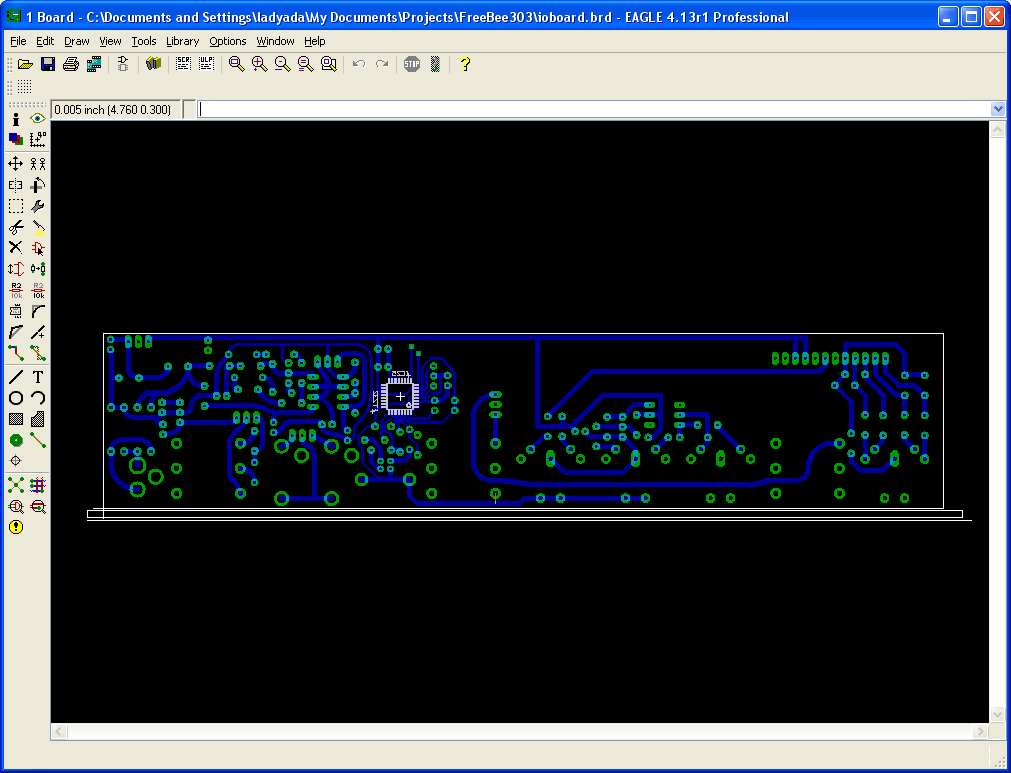
This is the PCB we'll be making a stencil for. It only has one chip but of course you can use a more complex layout
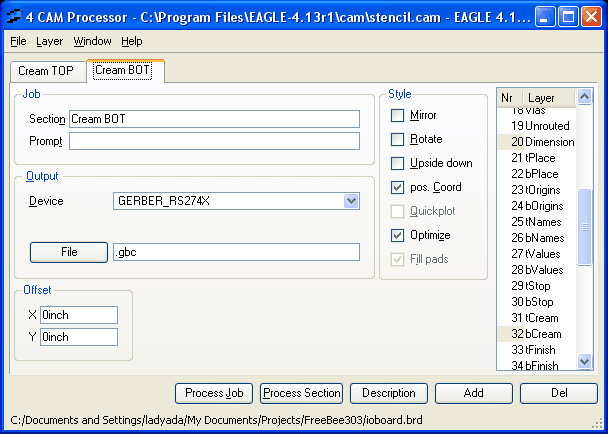
Your PCB software should be able to create/export the Cream Layer (solder paste layer) in Gerber RS274x format. In Eagle you can make your own Job for this quite easily
Also export the Dimension layer (PCB outline) since that will help a lot in registration
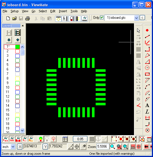
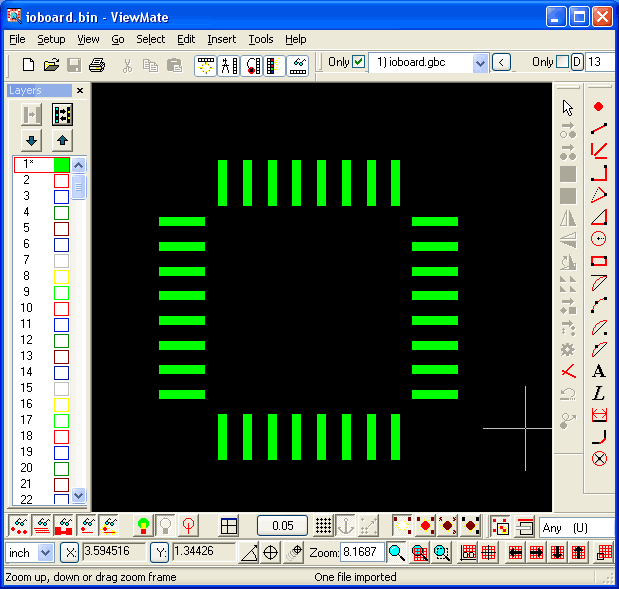
Import cream Gerber in ViewMate
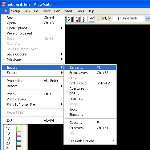
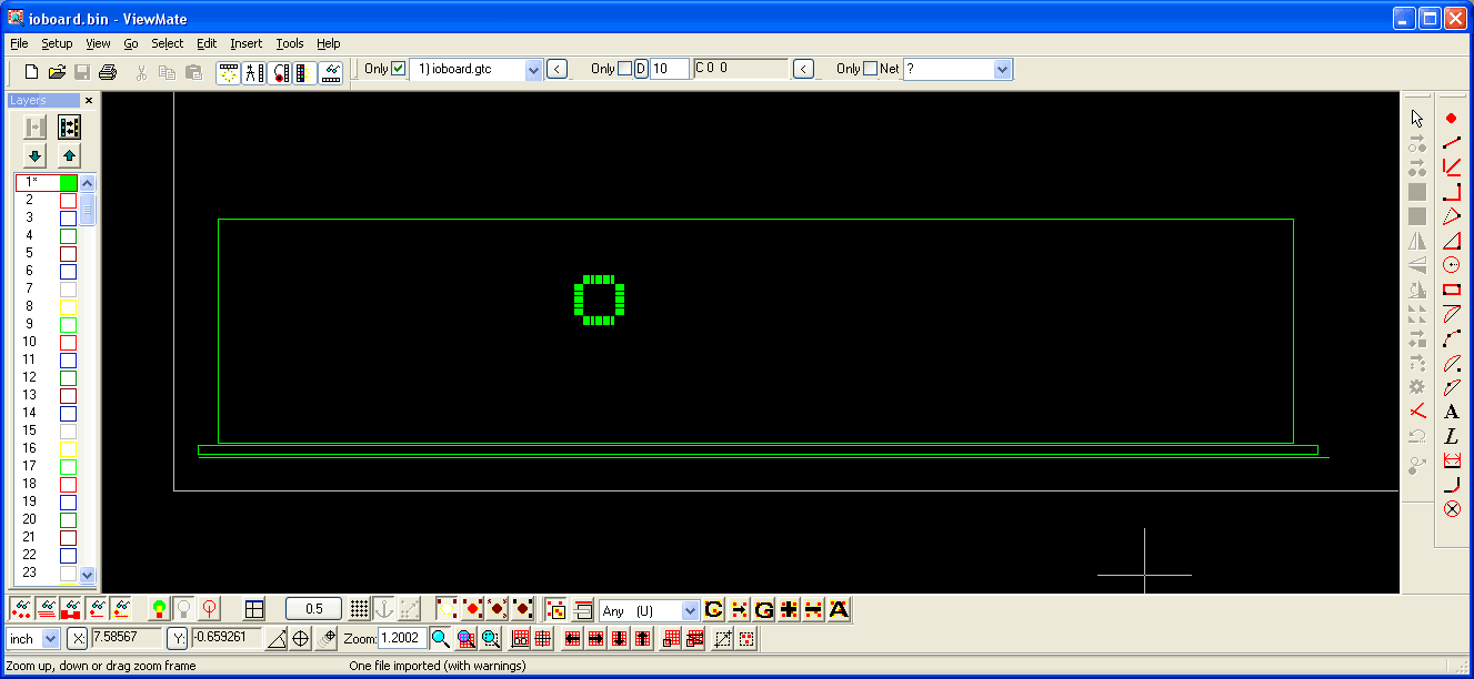
Start up ViewMate and File>Import>Gerber one of the Gerber files generated
You can zoom in using the Magnifying glass tool
Swell pads
Next we will make minor adjustnents to shrink the pads a little
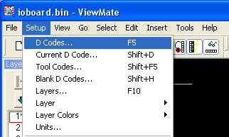
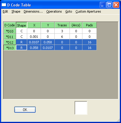
Select Setup>D Codes
Which will bring up a list of all the pads used. You will probably just want to select all of them
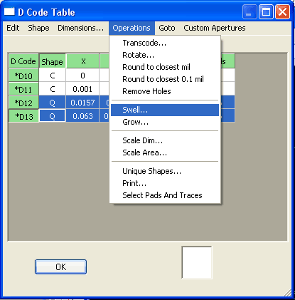
Then select Operations>Swell
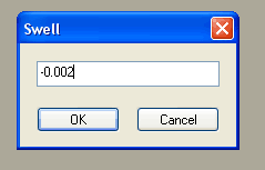
and input somewhere around -0.002 (2 mil) to shrink all the pads by 0.002 inches in each direction
You'll now see that your pads are thinner. This prevents bridging since the laser is not perfectly precise and tends to 'go over' the boundaries by a few mils.

