Table of Contents
The Voltage Controlled Oscillator
Schematic Overview:VCO
Inputs:
DigitalSequencer: Slide On/Off,Note
Outputs:
VoltageControlledFilter: Audio Out, MidiAndSync: CV Out
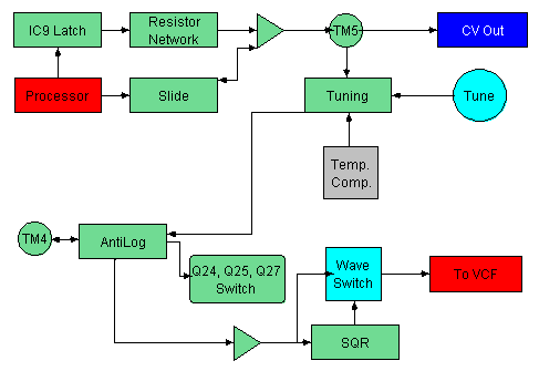
The VCO is comprised of 5 sections. The first of which is the Digital to Analog converter, which takes the digital signals for the note generated by the MicroProcessor and converts them to a voltage. After that the voltage is sent to a buffer and the Slide Circuit. Then it is sent to Q26 which is responsible for (blah… marked as "antilog" on the Tb303 block schematic). Q25 and Q27 act as a special switch, which is based on a Silicon Controlled Rectifier which, when coupled with an integrator, generates a Saw Wave. This waveform is then sent out to Q28 a 2SK30 JFET which is used as an operational amplifier. The output is sent to the switch, and also sent to Q8, where the saw wave is shaped into a square and back to the switch. From the switch, the output is sent to the VoltageControlledFilter
Block Diagram
The D/A converter and Resistor Network
The first part of this section is IC9, a 74ac174 Flip Flop, which takes 6 note inputs from Port C of the microcontroller and a clock signal (called Note Latch). On every clock signal, it samples the binary value from the note inputs, and outputs it to a 200K resistor network where it is added with the 5.333 Volt supply. This resistor network by virtue of math I do not understand takes the binary output of (for example) (010111, middle C) and mangles that into 3Volts. This of course, becomes the control Voltage.
The Slide Circuit And Buffer
I'm surprised no one wrote about this before, as it has a lot to do with slide time, and it's fairly simple to analyze.
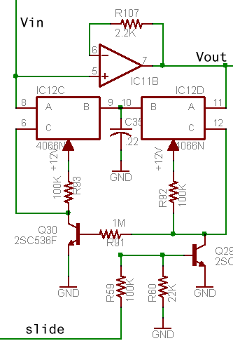
The noninverting op amp somehow works very well together with the DAC network to provide unity gain and buffering. That is… when the 4066 is turned off!
When SLIDE is HIGH, Q29 and Q30 are both turned on, and this should pull IC12C and IC12D closed (it is an analog switch chip) so that no signal flows through across the capacitor. This seemed a bit unusual to me because that means that slide would normally be high. So when SLIDE goes LOW, the transistors are turned off, allowing IC12C and IC12D to turn on, and allow the tuning voltage to flow across C35, making it lag if it changes. This creates a pitch sliding effect, instead of an instant change.
Oscillator Drift Compensation and Tuning
Anti-Log
Switch
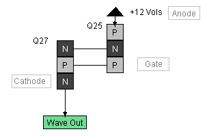
Transistors Q24, Q25 and Q27, along with C33 are responsible for generating the SawWave. The transistors Q25 and Q27 are set up in a special layout like so:
This arrangement is similar to a Silicon Controlled Rectifier.
From: Martin Czech martin.czech@intermetall.de,
WorkOnMe: This needs to be explained a little better and not be so copyright-infringey
And now to the SCR discharger:
As far as I can see the operation is as follows: Q24 is a saturated npn (diode), if a little leakage current flows through Q27, Q24 will establish a temp compensated base potential for Q25. This potential is about the emitter potential of Q24 + 0.6V. This is the reference potential for the whole SCR switch. The temperature compensation will prevent thermal run away of Q25. If the timing cap C33 is discharged by the expo converter such that the emitter junction of Q25 gets forward biased Q24 turns on and subsequently Q27, which in turn raises the base potential of Q25, this is the SCR snapback. The snapback point would depend on the thermal behavior of Q25 if there was not the temp compensation with Q24. If the SCR has triggered the base potential of Q25 rises to 12V (supply) minus the diode voltage of D25, ie. about 11.4V (this is possible because of R101, which disables the clamping action of Q24). I think the diode D25 is necessary to ensure that the SCR will turn off quite fast, because the emitter potential of Q25 has only to rise to 12V - 2x0.6V =10.8V to turn Q25 off. SCRs tend to not turn off, they are still on at very little currents, so I think the additional diode makes the shut off faster and safer.
I think the whole arrangement does only reach to the 12V supply because of the shut off latency of Q25 and Q27, these transistors are heavily saturated, it takes a lot of time to clear the base zone from all carriers. This also causes the flat portion of the saw wave and the time of this flatness should be independent of osc. frequency.
Could some 303 owner check this ?
I said that Q27 and Q25 are saturated when the SCR is on, ie. transistor beta will be very low, maybe 2 or 1.5 or so. This means that a large amount of the transistor current flows through the base, especially in the case of Q27 where there is no base resistance nor diode. If Q27 is not suited for such an application, it will sure burn out. Most good audio transistors with high Ft and high beta have shallow base junctions that are very sensitive. So the problem of Q27 burnout could be addressed with using (perhaps) lower beta, switch type transistor with very high specified max base current. The same applies to Q25 and Q24 (remember tempco compensation, Q25 and Q24 should be the same type)
Saw to Square Waveshaper
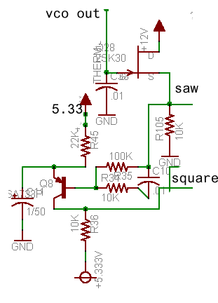
After the saw wave gets passed through the JFET and heads out to the waveform select switch, it heads into a jungle that I can only assume is a waveshaper. Here's a picture of the circuit:


