Cell phone jammers require a lot of power since the RF signal must be amplified a great deal: enough to drown out local tower signal and overload the analog front end of a cell phone. The basic design shown here has two oscillator/gain stages, for +25 dBm/+20dBm for the low and high channels: 300 mW/100mW = 0.4 Watts total output power spread over the bandwidth being jammed. Yet, in order to remain portable, the battery must be small and light. Therefore, a high power-density battery (such as Alkaline, NiMH or LiIon) is desirable. For the particular enclosure design here, I used a Li-ion/Li-Poly battery as it is thin enough to fit in between two of the circuit boards and maintain the desired form-factor.
Since there is a high current draw from the battery and these batteries are at risk for auto-combustion at such drains, a battery protection circuit (such as this one available for about $1.50 from batteryspace.com) OEM cell phone batteries have the protection circuitry built in and are a good low-cost replacement if purchased as surplus.
NiMH rechargeables and/or Alkaline 1.5V batteries are also a good choice as a battery as they have high power density, are less likely to explode, and are available everywhere. The input voltage should range between 3 to 5 volts so 2-3 Alkaline or 3-4 NiMH batteries will provide the best power arrangement. To get more power, do not use more batteries: above 5V input the circuit will not function correctly, instead use larger (alkaline AA, C, D or lead acid) batteries.
Each VCO/gainstage requires approximately 300mA at 3.6V (a standard cellphone arrangement will require two, for 600mA total) so whichever battery is chosen, it should be at least 1AH to be able to handle the high drain.
The USB/ttl converter (on the battery board) can be used to upload new firmware using the bootloader and view debug messages or possibly send commands.
The current design uses a FTDI FT232RL USB/serial converter chip. It's supported by every moden OS and looks like a serial port when plugged in. Other options are available, including the FT232BM (older gen, also SMT) or the MAX232 family serial level converters.
The main board is the workhorse of the RF jammer, comprising of the many powersupplies, digital/analog/PLL tuning circuitry, VCOs, and gain stages. The current layout is designed to be fab'd on standard FR4 0.062", a silkscreen may help placement, but it has been removed around the RF circuitry so that adding/moving the required passives around is easy. Thinner or different dielectric material may also be used, in which case the RF traces should be adjusted to maintain the correct stripline impedance (MEME link to impedance calcuator). Note that paper phenolic (cheap 'paper-layer' prototyping circuit boards) cannot be used.
In general, 1206 and SOIC components have been used whenever possible. In some cases, such as for the RF section, and certain components unavailable in SOIC, smaller parts such as TSSOP or 0603 have been used.
There are multiple power supplies, 3 DC/DC step-up converters and 2 linear drop outs. The 3 DC/DC stepups are for 5V, 12V, and 24V and are for powering the analog/RF system. The 2 LDOs are for 3.3 and 2.85V and are mostly used for the digital logic.
The 5V power supply is used to power the RF gain stages and provide a high enough voltage to guarantee proper input to the 2 LDOs. Each SXA-389B gain stage requires around 110mA at 5V and the LDO's will need around 10mA to power their subsections. If a different gain stage is to be used, the voltage and current requirements are likely to change and this stage should be redesigned. The current DC/DC converter used is the LM2733X which is inexpensive and high frequency.
The 12V supply is used to power the VCOs. The VCOs used here are high-power and require 25-40mA at 12V. A simple LT1301 is used, a high quality DC/DC converter that is pre-set for 12V. Other VCOs may require 8 or 5V in which case this stage may been to be redesigned to accomodate.
The 24V supply is to provide a high enough bias for the VCO control voltage. VCOs over require 12-28V bias voltages. A resistor divider sets the voltage, it should be high enough to provide a drop out (around 1V) above the highest voltage required but not be any higher than that. Only 1mA is required so it's not a particularly powerful supply. Currently an LT1173 is used, but this part is likely to be replaced by a less-expensive part in future revisions.
The 3.3V LDO powers the microcontroller, the waveform generator and the digital potentiometers. If the 5V supply is actually 5V (and not 6 or 7V) then the chip can be left out and 5V jumpered to the 3.3V. However, the 3.3V will be a little cleaner which may be desirable and all things being equal, it should probably be left in. A TI chip (the 27333 is used), but there are many other SOT23-5 pin compatible chips.
The 2.5V supply is for powering the PLL, which requires a <3V supply, if the PLL is not installed, dont install this supply.
The microcontroller is an essential component of this digitally-tuned jammer, even if the PLL is not used. It sets the digital potentiometers to adjust the bandwidth being jammed as well as creating the PWM output that sets the center frequency of the band. It also sets whether the jammer is working at high (20KHz) or low (100Hz) speed. If the PLL is installed, the micro will use it to fine-tune both the bandwidth and center frequency to assure the precise band is being jammed. The microcontroller also controls an LED to signal its current state to the user and operates the power switches (if they are being used) for each RF stage.
An ATmega88 is used, although an ATmega48 or 168 is pin and function compatible (just with less/more program storage). An ATmega8 is also acceptable although the firmware may need adjustments. The microcontroller is programmed through the 6-pin standard ISP header, and can also be programmed with a bootloader for firmware upgrades thru the USB port on the battery board. The microcontroller uses the onboard oscillator, so the fuses should be burned for the 8MHz internal oscillator.
Other microcontrollers (such as PIC, SX, etc) can theoretically be used, but as this one is inexpensive, has free development support and onboard PWM, it seems optimal.
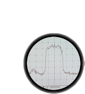
In order to sweep the VCO in a band, a sawtooth wave must be applied. A triangle wave may also be used: the effectiveness of different waveforms has not been analyzed but 'intuition' implies a sawtooth as ideal.
A common sawtooth circuit, a CMOS 555 current driving into a capacitor, is used. The frequency of the sawtooth can be adjusted, but examining 'professional' cell phone jammers has shown that most use 20KHz-200KHz oscillators. The frequency can be adjusted by manipulating a microcontroller pin that provides current to the transistor that forms the current source. if the pin is tied high, the 100ohm series resistor sets the frequency (20KHz). If the pin is pulled up thru a 100K pullup resistor (built into the microcontroller), the frequency goes down to about 100Hz. If the pin is pulled low, no current flows and the oscillator stops.
Once a sawtooth has been generated, it must be adjusted before feeding into the VCO. First the wave must be doubled: one for each VCO. Then, the peak-to-peak voltage for each must be adjusted so that the tuning voltage sweeps the desired bandwidth on that VCO. Finally a DC bias must be added to set the center frequency.
To generate the DC bias, the on-chip dual PWM is used. The PWM system has a maximum resolution of 10 bits but 8 bit accuracy seems sufficient. The PWM level is adjusted by assigning values to OCR1A / OCR1B. An LC (RC is also fine) network filters out the high frequency component.
To adjust the pp voltage, digital potentiometers are set up as variable voltage dividers: the wipers carrying the attenuated signal. 10K are specified but 1K are also good, although dissipate more power. The digital pots are SPI controlled and the microcontroller is used to set the values.
After attenuation, the DC bias is coupled in and there is a final gain/buffering stage. This stage amplifies both the DC bias as well as the gain. In theory, it would make sense to use the initial buffers as gain stages and then attenuate instead of attenuating and them amplifying. However, the restrictions of the digital potentiometers: they can only handle up to ~5V signals, requires the configuration used.
The final stage should be set so that the DC bias (3.3V or whatever the micro is running at) multiplied by the gain will not exceed Vtune of the VCO. This protects against damage to the most expensive component if the Wave Bubble is misconfigured and tries to drive a lower frequency VCO than expected.
An optional diode at the input to the VCO also protects against going below ground. An alternative is an approproately chosen zener diode configured as a clamp.