The first section of the main board to be assembled is the VCO (voltage controlled oscillator). This section converts a logarithmic voltage into a scaled oscillation. The relationship between the voltage and oscillation is called "1V/octave" because every 1V increase corresponds to a 1 octave increase in sound. For example, low C (65.4Hz) is generated by 2.0V, middle C (130.8Hz) is generated by 3.0V, and high C is generated by 4.0V.

Before: The VCO is in the top right corner of the mainboard

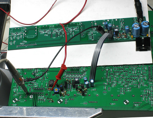
After: The completed VCO connected to the power supply. (The
jumper wire should be replaced with plain wire)
- The be sure not to confuse the 2SC536, 2SA733 and 2SK30 transistors, or the 2SC1583 and 2SC2291 matched pairs: they look similar. The PCB drawings of the 2SK30 show a filled in transistor, the drawing of the 2SA733 is hollow with a line through it, and the 2SC536 drawing is hollow.
- The resistors, thermistors, and non-electrolytic capacitors have no polarity. This is not true for the diodes, transistors, electrolytic capacitors, and op-amp. Putting them in backwards can destroy them.
- Both sides of the jumper J4 have a "1" printed next to the first pin, make sure that you have correctly corresponding pins connected.
- Don't forget that VR2 and SW1 are soldered on the top, opposite side of all the components.
- Solder in all parts except for S1 and VR2
- Solder in S1 and VR2 (on opposite side)
- Do basic calibration/testing.
The VCO can be simply tested without the use of an oscilloscope (although it helps a lot). The power supply 5.333V must be calibrated before this step:
- Apply power (make sure J4 is connected with wires)
- With the tuning knob VR2 centered, apply 2.0VDC using your powersupply to R89 (also pin 5 of IC11). Also center TM4 and TM5 to start.
- Use a multimeter with frequency-detection, or an oscilloscope, or a pair of cheap headphones, to probe pins 1 or 3 of the waveform switch. Switch between 2.0VDC and 3.0VDC to R89 while turning TM5 ('width') until the frequency at 3.0VDC is twice that of 2.0VDC.
- If you have an oscilloscope, verify also the offset voltages are
correct (Vmin = 6V for saw, 5V for square, Vmax = 11.5V for saw,
9V for square), if you have only a meter, the DC voltage should
be ~9V for saw ~7V for square, the AC voltage should be 5V for
saw, 4V for square.
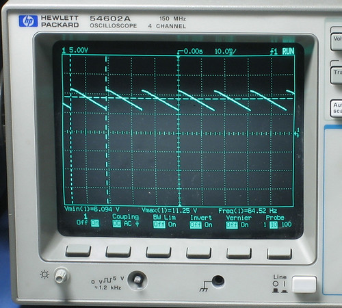
Tuning the sawtooth wave to C1. Note that the tip of the saw isnt 'sharp,' also the min and max voltages.
 >
>
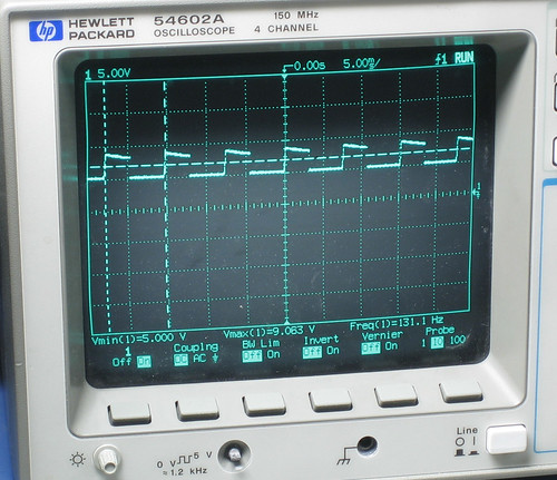
Tuning the square wave to C2. Note that the square wave droops slightly and isnt 50% duty cycle. - Now apply 2.0VDC to R89 and probe the waveform switch again, adjusting TM4 ('tune') until you see/hear C1, 65.4Hz.
The precise calibration step can be delayed until the rest of the synthesizer is completed, when you can just press a button to generate 2.0V and 3.0V to the VCO.
If you don't have a bench power supply you should center TM4 and TM5 (which will get you close enough) and listen to the square waveform using a pair of cheap headphones: probe the middle pin of the waveform switch while its set to SQR. Now touch the metal leads of the 200K resistors to vary the frequency and turn VR2 and note that the frequency changes.
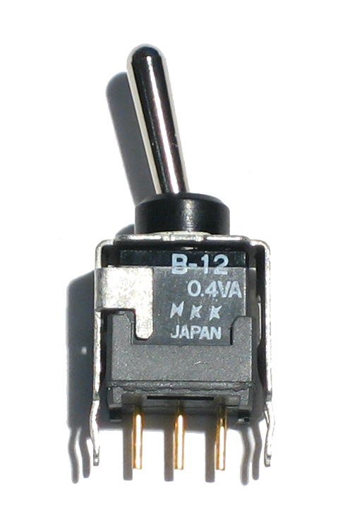 |
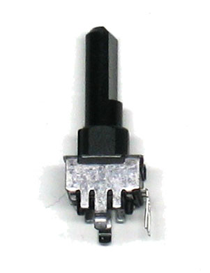
Toggle switch | 1 | SW1 | |||||||
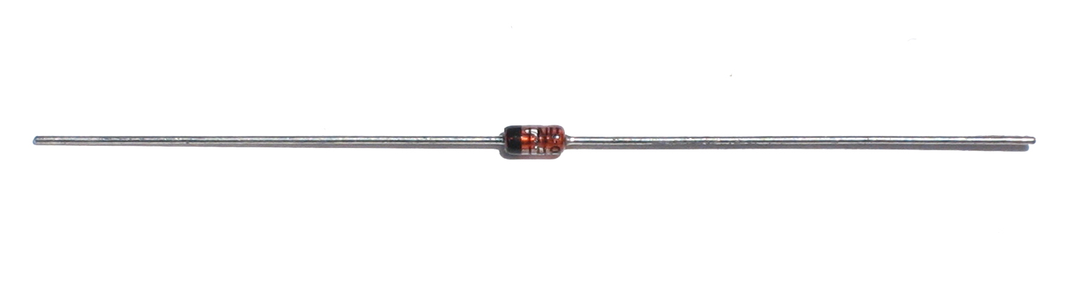 |
1N4148 | 3 | D25, D30, D31 | |||||||
|
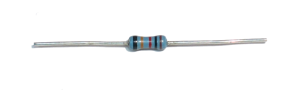
2.2K 5% resistor | 2 | R107, R104 | |||||||
|
10K 5% resistor | 4 | R34, R36, R105, R101 | |||||||
|
22K 5% resistor | 2 | R45, R60 | |||||||
|
100K 5% resistor | 6 | R35, R93, R92, R59, R102, R118 | |||||||
|
220K 5% resistor | 1 | R103 | |||||||
|
1MEG 5% resistor | 1 | R91 | |||||||
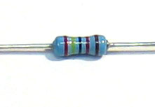 |
24.0K 1% resistor (red yellow black red brown) | 1 | R106 | |||||||
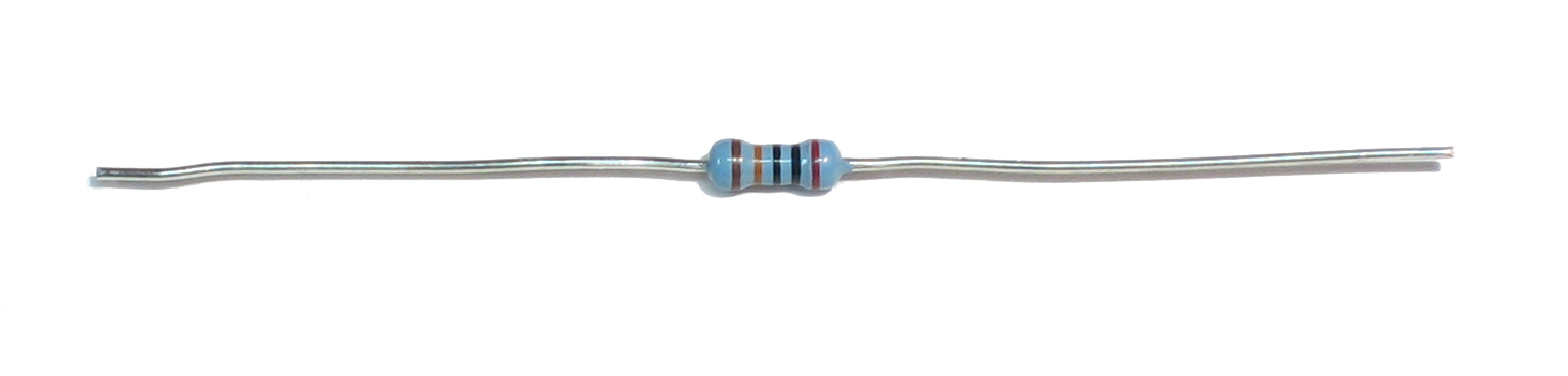 |
200K 1% resistor | 17 | R74-R90 | |||||||
 |
5K (502) trim potentiometer | 1 | TM5 | |||||||
|
50K (503) trim potentiometer | 1 | TM4 | |||||||
 |
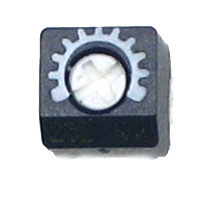
50K B (linear) potentiometer | 1 | VR2 | |||||||
 |
1K PTC Thermistor | 2 | R100A, R100B | |||||||
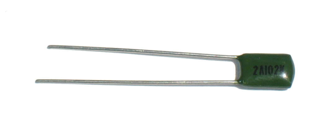 |
.001uF (2A102K) capacitor | 1 | C34 | |||||||
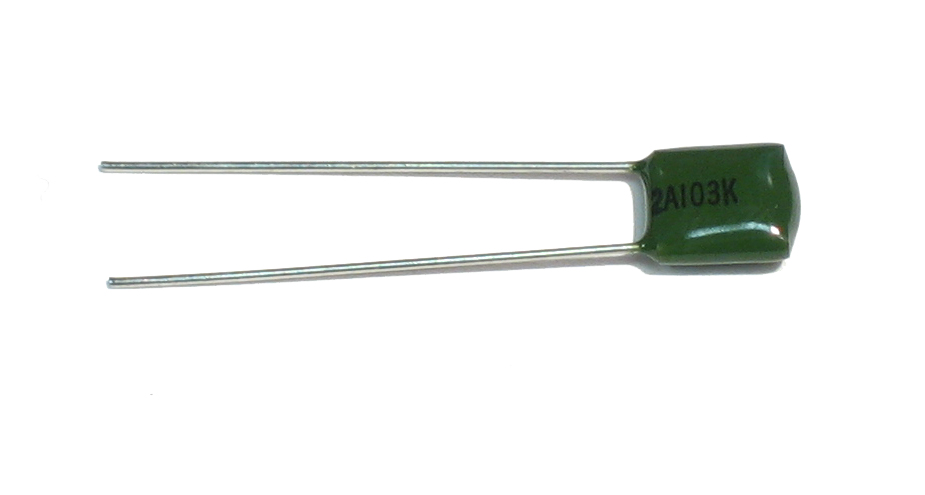 |
.01uF (2A103K) capacitor | 2 | C33, C10 | |||||||
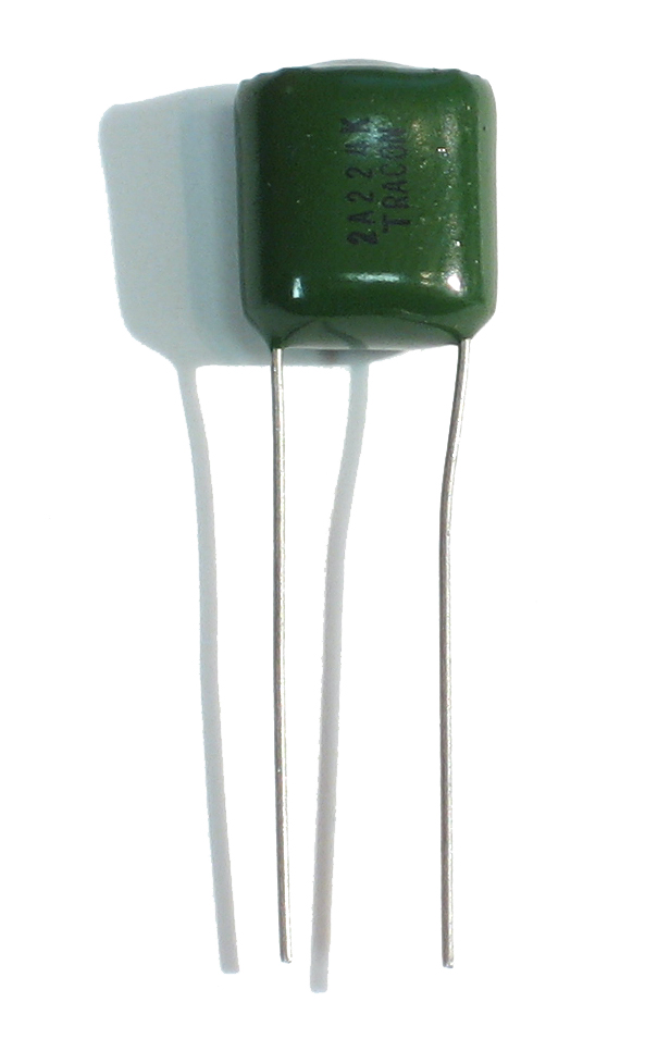 |
.22uF (2A224K) polyester capacitor | 1 | C35 | |||||||
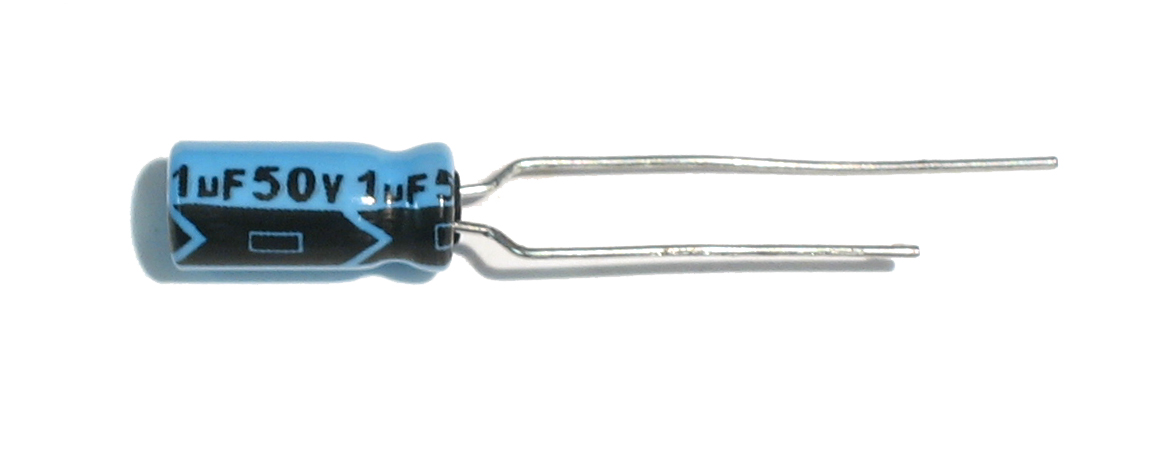 |
1uF electrolytic capacitor | 1 | C11 | |||||||
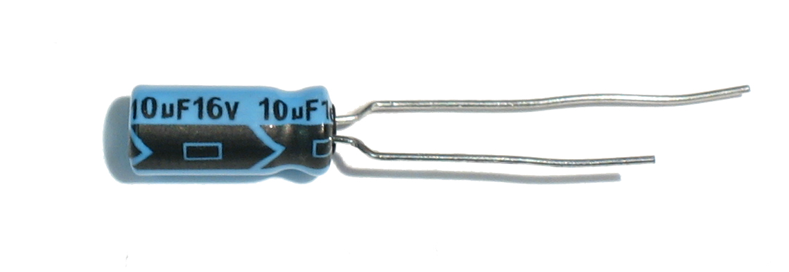 |
10uF electrolytic capacitor | 2 | C31, C32 | |||||||
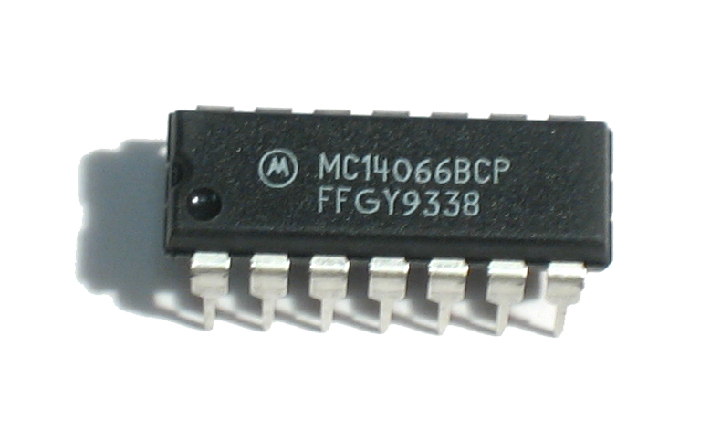 |
4066 analog switch | 1 | IC12 | |||||||
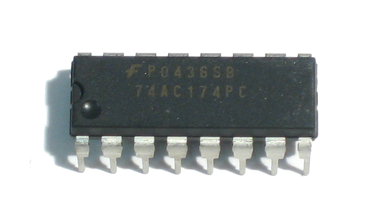 |
74AC174 | 1 | IC9 | |||||||
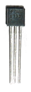 |
2SA733P, TO-92 PNP transistor | 2 | Q8, Q27 | |||||||
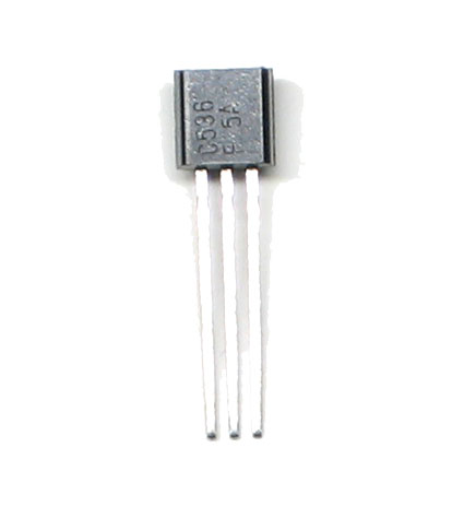 |
2SC536F, TO-92 NPN transistor | 4 | Q29, Q30 , Q25 , Q24 | |||||||
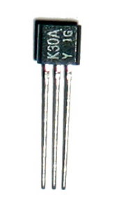 |
2SK30 JFET, 2SK30AO sub-type if there is one | 1 | Q28 | |||||||
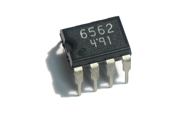 |
AN6562 8-DIP dual Op-Amp | 1 | IC11 | |||||||
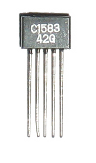 |
2SC1583 5-SIP matched pair with common emitter | 1 | Q26 |

